

Light Sources for Lithography Market Projected to Reach USD 4.3 Billion by 2034 Driven by EUV Adoption in Advanced Semiconductor Nodes
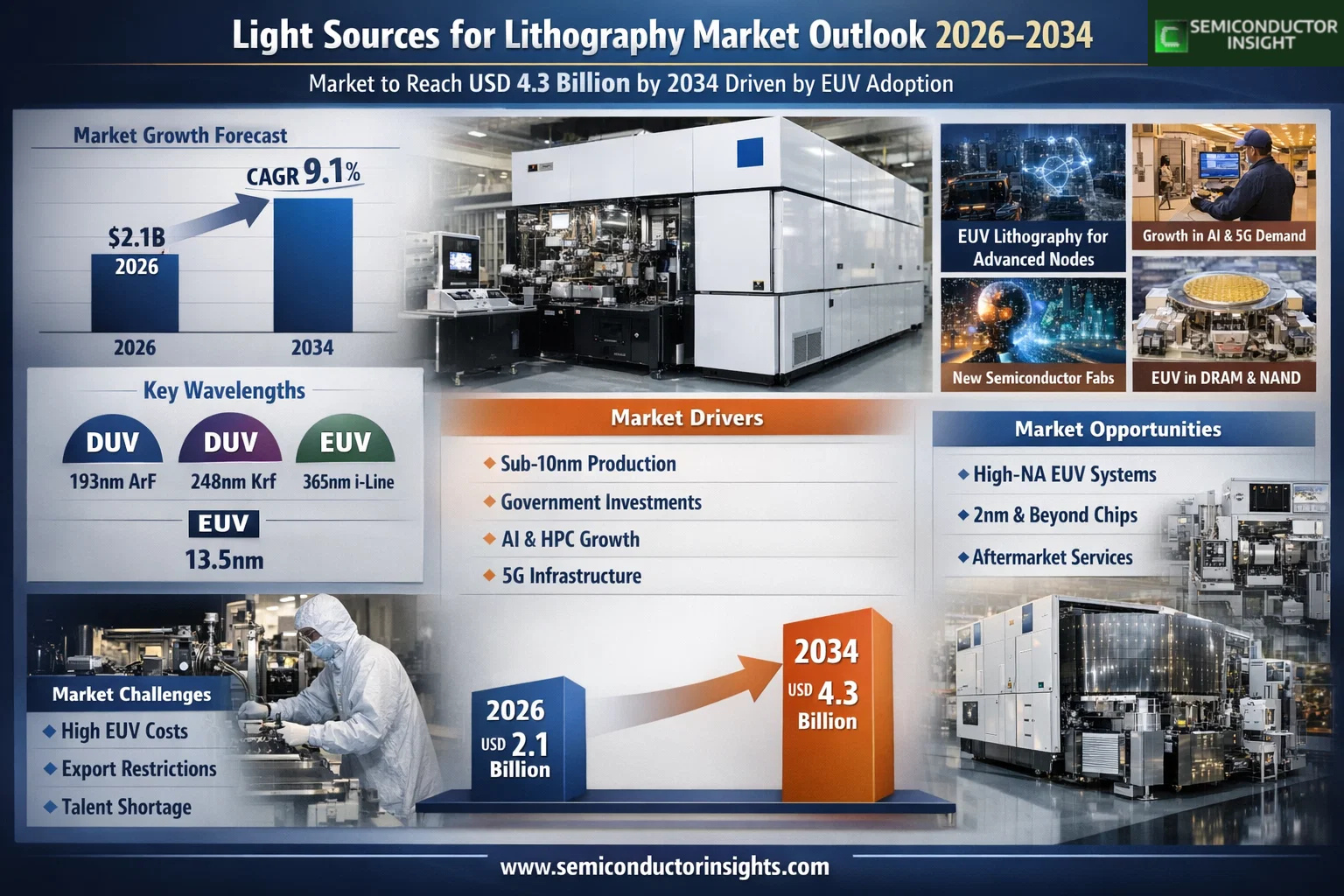
Global Light Sources for Lithography Market was valued at USD 2.1 billion in 2026 and is projected to reach USD 4.3 billion by 2034, growing at a CAGR of 9.1% during the forecast period 2026–2034. Market expansion is being guided by steady technology-node migration and increased deployment of extreme ultraviolet systems across advanced semiconductor manufacturing lines.
Light sources for lithography are core subsystems in semiconductor fabrication equipment used to transfer circuit patterns onto wafers with nanometer-level precision. These sources generate ultraviolet radiation at defined wavelengths, including deep ultraviolet (DUV) such as ArF (193nm), KrF (248nm), and i-line (365nm), as well as extreme ultraviolet (EUV) at 13.5nm. Selection of wavelength and source power directly influences resolution, throughput, and process control in logic, memory, and specialty device production.
👉 Access the complete industry analysis and demand forecasts here: https://semiconductorinsight.com/report/light-sources-for-lithography-market/
Market Definition and Dynamics
The market is evolving alongside the global semiconductor industry’s transition toward sub-10nm and emerging sub-3nm process technologies. As device geometries shrink, lithography systems require higher source brightness, tighter wavelength stability, and improved uptime. EUV light sources are increasingly deployed in leading-edge logic and memory production, while DUV platforms continue to support high-volume manufacturing at mature and mid-range nodes.
Capacity expansion programs, regional semiconductor self-sufficiency initiatives, and process complexity growth are reinforcing long-term demand. Equipment ecosystems are becoming more integrated, with light source performance closely tied to scanner productivity, overlay control, and yield management across advanced fabs.
Market Drivers
- Rising production at below-10nm nodes requiring EUV lithography and high-power, high-stability light sources
- Government-backed semiconductor manufacturing programs increasing new fab and tool investments
- Expanding use of advanced chips in AI, high-performance computing, and 5G infrastructure
- EUV adoption extending from logic devices into DRAM and advanced NAND manufacturing
Market Restraints
- High capital cost and operating complexity of EUV light source systems
- Export controls and technology transfer restrictions affecting tool shipments and service models
- Limited availability of specialized engineering talent in plasma, laser, and precision optics domains
Market Opportunities
- Commercial rollout of High-NA EUV platforms enabling patterning at 2nm and below
- Growth in aftermarket services, modules, and consumables tied to installed base expansion
- Power and efficiency improvements in next-generation DUV and EUV source architectures
Competitive Landscape
The competitive landscape is concentrated among a limited number of highly specialized laser and plasma light source providers with deep integration into lithography tool platforms. Competition centers on source power, uptime, maintenance intervals, and field service capability. Strategic partnerships with scanner manufacturers and leading-edge fabs remain central to market positioning.
Key suppliers include subsidiaries and partners of ASML such as Cymer, along with Japan-based Gigaphoton and other regional technology developers.
List of Key Light Sources for Lithography Companies
- Cymer (ASML)
- Gigaphoton
- Beijing RSLaser Opto-Electronics Technology
- Optosystems
- USHIO
Segment Analysis
By Type
- DUV Light Sources (ArF, KrF, i-line)
- EUV Light Sources
- Others
By Application
- Integrated Device Manufacturers (IDM)
- Foundry
- Others
Regional Insights
Asia-Pacific leads global demand, supported by large-scale foundry and memory manufacturing capacity and continued fab investments across China, Taiwan, South Korea, and Japan. North America remains a major innovation and adoption center for EUV platforms, supported by domestic manufacturing incentives and advanced node development programs. Europe holds a critical technology position through lithography ecosystem leadership and component manufacturing depth. South America and Middle East & Africa represent emerging markets, with activity focused on mature-node production, specialty semiconductors, and long-term capability building.
📄 Download a free sample to explore segment dynamics and competitive positioning: https://semiconductorinsight.com/download-sample-report/?product_id=107973
About Semiconductor Insight
Semiconductor Insight is a global intelligence platform delivering data-driven market insights, technology analysis, and competitive intelligence across the semiconductor and advanced electronics ecosystem. Our reports support OEMs, investors, policymakers, and industry leaders in identifying high-growth markets and strategic opportunities shaping the future of electronics.
🌐 https://semiconductorinsight.com/
🔗 LinkedIn: Follow Us
📞 International Support: +91 8087 99 2013
