

ArF Lithography Market Poised for Precision Growth to Reach USD 1.6 Billion
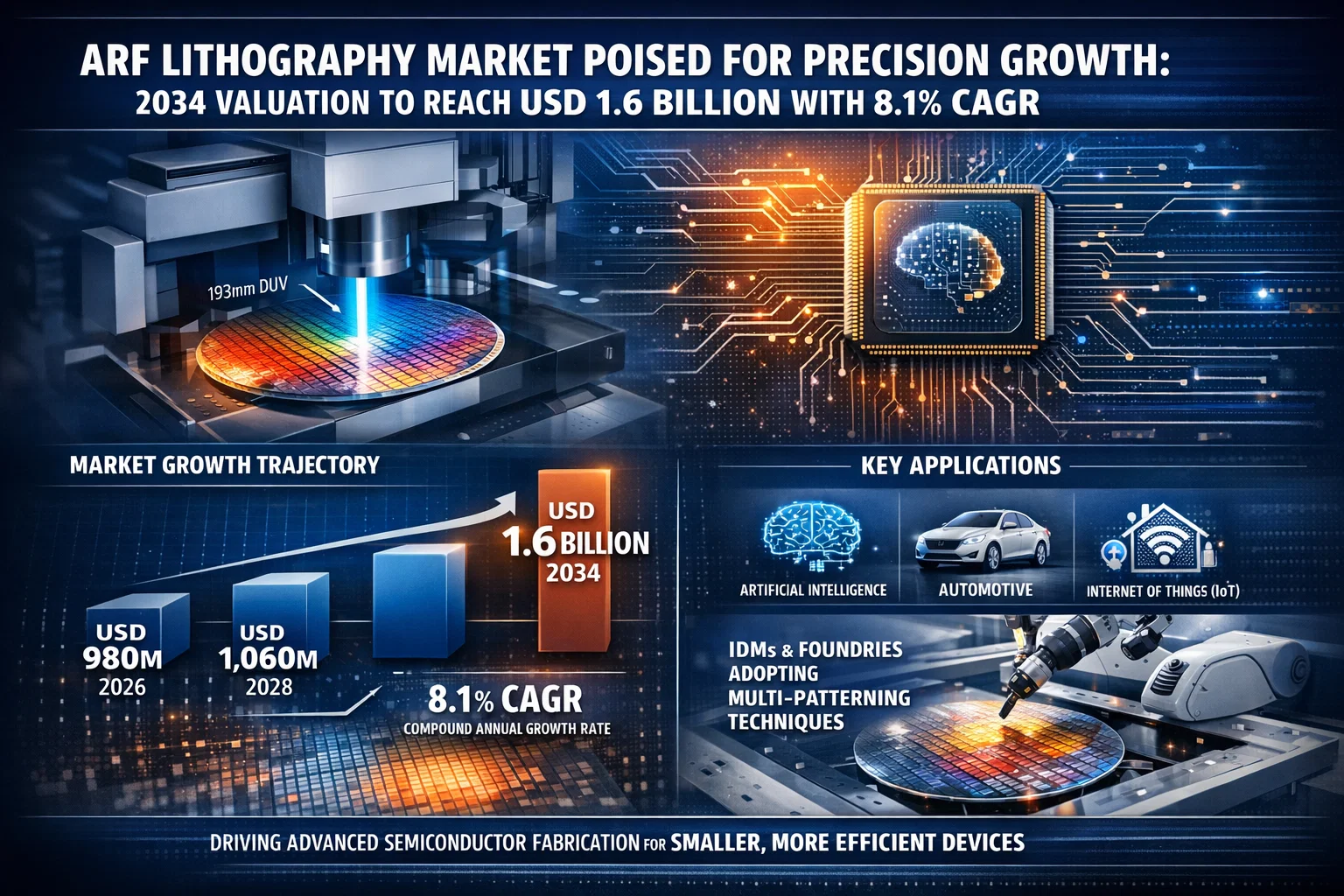
Global ArF Lithography market, valued at USD 980 million in 2026, is projected to grow from USD 1,060 million in 2026 to USD 1,606 million by 2034. This steady trajectory is underpinned by an 8.1% CAGR, driven by the relentless demand for smaller, more efficient semiconductor devices across the AI, automotive, and IoT sectors.
Market Segmentation:
ArF (Argon Fluoride) lithography represents the "high-resolution" engine of modern semiconductor fabrication. By utilizing 193nm deep ultraviolet (DUV) light, these systems enable the intricate patterning required for sub-30nm nodes. The leap toward a USD 1.6 billion valuation by 2033 reflects a strategic pivot as Integrated Device Manufacturers (IDMs) and Foundries leverage multi-patterning techniques to extend the life and precision of DUV technology in an increasingly complex chip architecture landscape.
Download Full Report: https://semiconductorinsight.com/report/arf-lithography-market-size/
Market Dynamics
Drivers
- Surging Demand for Advanced Nodes: The transition to sub-20nm processes for smartphones and AI accelerators is fueling the adoption of ArFi (Immersion) systems, which offer superior resolution and yield rates.
- Dominance of Analog Chip Production: ArF systems remain the "sweet spot" for analog and mixed-signal ICs, balancing nanometer-level precision with the cost-effectiveness required for power management and RF components.
Challenges & Restraints
- Geopolitical & Supply Chain Pressures: With China holding a 53% market share, international trade regulations and data sovereignty issues regarding high-end lithography equipment remain significant operational hurdles.
- Extreme Technical Integration: The backend complexity of immersion lithography, including sophisticated fluid dynamics and overlay performance, presents steep barriers for new market entrants.
Strategic Segmentation
The ArF Lithography market is categorized by high-growth technological and application-specific segments:
- By Type:
- ArFi Immersion Lithography (54% Share): The dominant segment for advanced node semiconductors.
- ArF Dry Lithography (46% Share): Critical for mature nodes and cost-sensitive applications.
- By Application:
- Analog Chips (Lead Segment): Essential for automotive and industrial power management.
- Logic Chips, Optical Sensors, and others.
- By End User:
- IDM (65% Share): Vertically integrated manufacturers leading strategic equipment investments.
- Foundries (35% Share) and Research Institutions.
- By Technology Node:
- 20-28nm: The optimal balance for mainstream ICs and automotive semiconductors.
- Below 20nm and 28-45nm nodes.
Competitive Landscape
The competitive environment is highly consolidated, with three major players—ASML, Nikon, and SMEE—collectively holding 100% of the market share. As of 2026, these leaders are focusing on improving throughput and overlay metrics to support the global surge in foundry capacity.
Key Industry Participants:
- ASML Holdings NV (Netherlands)
- Nikon Corporation (Japan)
- Shanghai Micro Electronics Equipment (SMEE) (China)
- Canon Inc. (Japan)
- Tokyo Electron Limited (Japan)
- Lam Research (U.S.)
- Applied Materials (U.S.)
- KLA Corporation (U.S.)
Download Full Report: https://semiconductorinsight.com/report/arf-lithography-market-size/
Download Sample Report: https://semiconductorinsight.com/download-sample-report/?product_id=91104
About Semiconductor Insight
Semiconductor Insight is the world's leading provider of market intelligence for galvanic isolation, power management, and serial communication components. We provide the technical data and strategic foresight needed to design the safe, connected systems of the 2030s.
Website: https://semiconductorinsight.com/
LinkedIn: Follow Us
International Support: +91 8087 99 2013
